

 Manufacturers
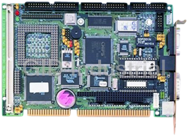
ADVANTECH PCM-6135

Description
Advantech PCM-6135 CPU Card - Half-size 386-chip All-in-one CPU Card with VGA CRT/LCD, SSD
Part Number
PCM-6135
Price
Request Quote
Manufacturer
ADVANTECH
Lead Time
Request Quote
Category
Single Board Computers
Specifications
Form Factor
PC/104
BIOS
AMI 128 KB Flash memory
CPU with core logic
ALi M6117, 40 MHz 80386SX CPU
Enhanced IDE hard disk drive interface
Supports up to two Enhanced IDE devices. BIOS auto-detect
Floppy disk drive interface
Supports up to two FDDs: 3.5" (720KB or 1.44MB) and/or 5.25" (360KB or 1.2MB)
Multimode parallel port
Configured to LPT1, LPT2, LPT3 or disabled. Supports SPP/EPP/ECP; D-SUB 25-pin connector on board.
PS/2 keyboard connector
Mini-DIN keyboard connector
RAM
Two 72-pin SIMM socket. Supports standard page mode/EDO DRAM from 1 to 32 MB (accepts 1, 4, 16 MB modules)
Serial ports
One serial RS-232 port, one serial RS-232/422/485 port. Two 16C550 compatible UARTs
SSD
3 sockets for a 360 KB/1.44 MB Flash/RAM/ROM disk and 1 socket for DiskOnChip 2000 Flash disk
Features
- AMI BIOS for enhanced system performance
- Built-in 100% PC/AT compatible 80386SX CPU with core logic
- Built-in enhanced IDE hard disk drive interface
- Compact size (185 mm x 122 mm).
- ISA-bus expansion with on-board PC/104 modules
- ISA-bus SVGA/LCD display controller (LCD, EL and CRT displays) plus on-board DB-15 connector (PCA-6135 only)
- Lithium battery backup for real-time clock/calendar
- On-board PS/2 keyboard connector
- One multimode parallel port supporting SPP/ECP/EPP
- PC/104 connection supports face-up installation
- Single voltage power requirement (+5 V @ 2.0 A)
- Two serial ports: one RS-232 and one RS-232/422/485; on-board DB-9 connector is designated as COM1
- Up to 32 MB DRAM
- Watchdog timer, interval 1~63 seconds
Datasheet

Extracted Text
PCM-3350 Series
User's Manual
LAN Interface
CPU Module with SVGA/LCD/
NS Geode 586-Level PC/104
Copyright notice
This document is copyrighted, 2001, by Advantech Co., Ltd. All rights
are reserved. The original manufacturer reserves the right to make
improvements to the products described in this manual at any time
without notice.
No part of this manual may be reproduced, copied, translated or
transmitted in any form or by any means without the prior written
permission of the original manufacturer. Information provided in this
manual is intended to be accurate and reliable. However, the original
manufacturer assumes no responsibility for its use, nor for any
infringements upon the rights of third parties which may result from its
use.
Acknowledgements
AMD is a trademark of Advanced Micro Devices, Inc.
Award is a trademark of Award Software International, Inc.
Cyrix is a trademark of Cyrix Corporation.
IBM, PC/AT, PS/2 and VGA are trademarks of International Business
Machines Corporation.
Intel and Pentium are trademarks of Intel Corporation.
®
Microsoft Windows is a registered trademark of Microsoft Corp.
RTL is a trademark of Realtek Semiconductor Co., Ltd.
C&T is a trademark of Chips and Technologies, Inc.
UMC is a trademark of United Microelectronics Corporation.
Winbond is a trademark of Winbond Electronics Corp.
STPC is a trademark of SGS Thomson Corp.
For more information on this and other Advantech products, please
visit our website at: http://www.advantech.com
For technical support and service, please visit our support website at:
http://www.advantech.com/support
This manual is for the PCM-3350P, PCM-3350F.
Part No. 2006335052
3rd. Edition Printed in Taiwan June, 2002
Packing list
Before you begin installing your card, please make sure that the
following materials have been shipped:
1 PCM-3350 All-in-one single board computer
1 Start-up manual
CD-ROM or Disks for utility, drivers, and manual (in PDF format)
1 2.5" IDE flat cable, 44-pin to 44-pin (product no. 1701440350)
1 PS/2 keyboard & mouse cable (product no. 1700060202)
2 serial port cables (product no. 1700100250)
1 cable 6P - 6P (product no. 1703060053)
1 parallel cable (product no. 1700260250)
1 26-34 pin FDD cable converter (product no. 9681000044)
1 floppy cable, for 3.5" FDD only (product no. 1701340501)
1 FDD flat cable (product no. 1906000001)
1 VGA cable (product no. 1701160150)
1 LAN cable (product no. 1701100202)
If any of these items are missing or damaged, contact your distributor
or sales representative immediately.
Contents
Chapter 1 General Information 1
1.1 Introduction....................................................................... 2
1.2 Features ............................................................................. 3
1.3 Specifications .................................................................... 4
1.3.1 Standard SBC functions .............................................. 4
1.3.2 VGA function .............................................................. 4
1.3.4 Ethernet function ........................................................ 5
1.3.5 Solid state disk ............................................................. 5
1.3.6 Mechanical and environmental .................................... 5
1.4 Board dimensions ............................................................ 6
Chapter 2 Installation 7
2.1 Connectors ....................................................................... 8
2.2 Locating connectors ........................................................ 9
2.3 Safety precautions .......................................................... 10
2.4 Ethernet connector (CN1) (PCM-3350F/N only)...... 10
2.4.1 Ethernet connector (CN1).........................................10
2.4.2 Network boot............................................................. 10
2.5 LCD display connector (CN2)...................................... 10
2.6 Serial ports
(CN3: COM1; CN4: COM2/RS-232;
CN18: COM2/RS-422/485) ......................................... 11
2.6.1 RS-232 connection (COM1: CN3) ............................ 11
2.6.2 RS-232/422/485 connection
(COM2: CN4: RS-232; CN18: RS-422/485) ..................... 11
2.7 EIDE HDD connector (CN5) ....................................... 12
2.7.1 Connecting the hard drive ......................................... 12
2.8 PC/104 connector (CN6) ............................................... 12
2.9 Parallel port connector (CN7) ...................................... 13
2.10 Backlight connector (CN8)........................................... 13
2.11 VGA connector (CN9) ................................................... 13
2.11.1 CRT display connector (CN9) ................................. 13
2.12 Main power (+5 V / +12 V) connector (CN11) .......... 13
2.13 PS/2 keyboard/mouse connector (CN12) ................... 14
2.14 FDD connector (CN14) ................................................. 14
2.14.1 Connecting the floppy drive ..................................... 14
2.15 CompactFlash™ socket (CN16) .................................. 15
2.16 USB connector (CN17) ................................................. 15
2.17 Multifunction Jumpers (MJ1)...................................... 16
2.16.1 Auxilary power connector (MJ1-A) ........................ 16
2.17.2 Fan connector (MJ1-B) ........................................... 17
2.17.3 Reset button connector (MJ1-C)............................. 17
2.17.4 IR connector (MJ1-D) ............................................ 17
2.17.5 Watchdog timer configuration (MJ1-E) ................... 17
2.18 SO DIMM socket (Slot1) ............................................. 18
2.18.1 Installing SODIMMs ............................................... 18
Chapter 3 Software Configuration 21
3.1 Introduction..................................................................... 22
3.2 Utility CD disk ................................................................ 22
3.3 VGA display software configuration ............................ 22
3.4 Connections for two standard LCDs........................... 24
3.4.1 Connections for Toshiba LTM10C042(640 x 480 TFT
color LCD) ......................................................................... 24
3.4.2 Connections for Toshiba LTM12C275A
(800 x 600 TFT color LCD) .............................................. 25
Chapter 4 Award BIOS Setup 27
4.1 System test and initialization ........................................ 28
4.1.1 System configuration verification .............................. 28
4.2 Award BIOS setup ......................................................... 29
4.2.1 Entering setup ............................................................ 29
4.2.2 Standard CMOS setup .............................................. 30
4.2.3 BIOS features setup..................................................31
4.2.4 Chipset features setup ............................................... 32
4.2.5 Power management setup .........................................33
4.2.6 PnP/PCI configuration .............................................. 34
4.2.7 Integrated peripherals ................................................ 35
4.2.8 Change password ...................................................... 36
4.2.9 Save & exit setup ...................................................... 37
4.2.10 Exit without saving .................................................. 37
Chapter 5 PCI Bus Ethernet Interface 39
5.1 Introduction..................................................................... 40
5.2 Installation of Ethernet driver ..................................... 40
5.2.2 Installation for Windows 98/2000 .............................. 41
5.3 Further information ........................................................ 44
Chapter 6 SVGA Setup 45
6.1 Introduction..................................................................... 46
6.1.1 Chipset ....................................................................... 46
6.1.2 Display memory ........................................................ 46
6.2 Installation of SVGA driver .......................................... 46
6.2.1 Installation for Cyrix MediaGX Certified drivers for
Windows 95/98. Insert the disk into the CD-ROM drive. .. 47
6.2.2 Installation for Windows NT ..................................... 50
6.3 Further information ........................................................ 56
Appendix A Programming the Watchdog Timer 57
A.1 Programming the watchdog timer ............................... 58
Appendix B Installing PC/104 Modules 61
B.1 Installing PC/104 modules ............................................ 62
Appendix C Pin Assignments 65
C.1 Ethernet connector (CN1) ............................................ 66
C.2 LCD connector (CN2) ................................................... 67
C.3 COM1 connector (CN3) ............................................... 68
C.4 COM2 connector (CN4) ............................................... 68
C.5 EIDE hard drive connector (CN5) .............................. 69
C.6 PC/104 connector (CN6) ............................................... 70
C.7 Parallel port connector (CN7) ...................................... 70
C.8 Backlight connector (CN8)........................................... 71
C.9 VGA connector (CN9) ................................................... 71
C.10 Main power (+5 V) connector (CN11) ........................ 72
C.11 PS/2 keyboard/mouse connector (CN12) ................. 72
C.12 FDD connector (CN14) ................................................. 73
C.13 CompactFlash™ socket (CN16) .................................. 74
C.14 COM2 connector for 422/485 (CN18) ........................ 76
C.15 Multifunction Jumpter (MJ1) ...................................... 76
Appendix D System Assignments 79
D.1 System I/O ports ............................................................ 80
D.2 DMA channel assignments........................................... 81
D.3 Interrupt assignments ................................................... 82
D.4 1st MB memory map ..................................................... 83
Appendix E LCD Services 85
E.1 LCD services .................................................................. 86
Figures
Figure 1-1: PCM-3350 dimensions................................................................6
Figure 2-1: Locating connectors (component side) ..................................... 9
Figure 2-2: Locating connectors (solder side) ............................................. 9
Figure 3-1: Contents of the PCM-3350 Series utility disk22
Figure 3-2: BIOS VGA setup screen23
Figure 4-1: BIOS setup program initial screen29
Figure 4-2: CMOS setup screen30
Figure 4-3: BIOS features setup31
Figure 4-4: Chipset features setup32
Figure 4-5: Power management setup33
Figure 4-6: PnP/PCI configuration34
Figure 4-7: Integrated peripherals35
Figure B-1: PC/104 module mounting diagram63
Figure B-2: PC/104 module dimensions (mm) (±0.1).................................63
Figure C-1: CompactFlash™ socket............................................................75
...........................................
................................................................
................................................................
.........................................................
...............................................................
...................................................................
...................................................................
.............................................
..............................................................
.............................
Tables
Table 2-1: Connectors8
T11
Table 2-3: Serial port default settings12
T64
able C-1: Ethernet connector (CN1)T66
67T
T68
T68
T69
T70
Table C-9: VGA connector (CN171
able C-8: Backlight connector (CN8)T71
Table C-10: Main power (+5 V) connector (CN172
1: PS/2 keyboard/mouse connector (CN12)able C-1T72
T73
T74
able C-14: COM2 connector for 422/485 (CN18)T76
able C-15: MJ1-A, -5 V,T -12 V input76
Table C-16: MJ1-B, fan connector76
77T
able C-19: MJ1-E, watchdog jumperT77
77T
T80
T81
able D-3: Interrupt assignmentsT82
83T
able D-4: 1st MB memory map......................................................................................
...................................................................................
...........................................................................able D-2: DMA channel assignments
...........................................................................................able D-1: System I/O ports
.....................................................................................able C-17: MJ1-C, reset button
............................................................................
able C-18: MJ1-D, IR connector....................................................................................
.................................................................................
.............................................................................
........................................................
.................................................................able C-13: CompactFlash™ socket (CN16)
...............................................................................able C-12: FDD connector (CN14)
...................................................
........................................................1)
............................................................................
................................................................................1)
.......................................................................able C-7: Parallel port connector (CN7)
.................................................................able C-5: EIDE hard drive connector (CN5)
................................................................................able C-4: COM2 connector (CN4)
................................................................................able C-3: COM1 connector (CN3)
....................................................................................able C-2: LCD connector (CN2)
.............................................................................
...........................................................able B-1: PCM-3350 PC/104 connectors (CN6)
............................................................................
........................................................able 2-2: Serial port connections (COM1, COM2)
......................................................................................................
1
General Information
This chapter gives background information on
the PCM-3350.
Sections include:
Introduction
Features
Specifications
Board dimensions
CHAPTER
1.1 Introduction
The PCM-3350 is the ultimate cost-effective solution for limited space
applications. It is a new NS Geode Biscuit PC with enhanced graphics
function. It uses a NS CS5530A chipset which supports TFT LCDs. It
offers all the functions of an AT-compatible industrial computers on a
single board. The PCM-3350 comes with an embedded high-perfor-
mance GX1-300 processor on-board. For maximum performance, the
PCM-3350 Series also supports an SDRAM SODIMM socket that can
accept up to 128 MB memory.
On-board features include an Ethernet interface, socket for Compact
Flash Card, Enhanced IDE interface with up to Ultra DMA transfer
protocol, one parallel port, two serial ports (RS-232 and RS-232/422/
485) and a PS/2 keyboard/mouse interface. A SVGA/LCD display
controller (LCD, and CRT displays) allows LCD screen resolutions up
to 1024 x 768 and CRT resolutions up to 1280 x 1024 @ 16 colors.
The PCM-3350 complies with the "Green Function" standard and
supports three types of power saving features: Normal, Doze, and
Sleep modes.
The display type configuration is done through the software. A single
Flash chip holds the system BIOS and the VGA BIOS. This minimizes
the chip usage and eases configuration. You can change the display
BIOS simply by programming the Flash chip.
If you need additional functions, the PCM-3350 has a PC/104 connec-
tor for future upgrades.
2 PCM-3350 User's Manual
1.2 Features
Ultra-compact size single board computer, smaller than a 3½" hard
disk drive (96 mm x 90 mm)
Onboard NS Geode GX1 300MHz CPU
Up to 128 MB system memory, by way of SODIMM (SDRAM)
Onboard VGA/18-bit LCD interface
Supports CompactFlash card
Built-in Enhanced IDE (AT bus) hard disk drive interface
Onboard PS/2 keyboard/mouse connector
Two serial ports (RS-232)
Upgradeable through PC/104 module
Green engine with sleep mode and low power consumption
+5 V power supply (for CPU board), +12 V power supply (for PC/104,
backlight)
Onboard 10/100Base-T Ethernet interface
Chapter 1 General Information 3
1.3 Specifications
1.3.1 Standard SBC functions
CPU:
Embedded Low power NS Geode GX1-300 MHz processor
BIOS: AWARD 256 KB Flash memory
System memory: One 144-pin SODIMM socket accepts up to 128
MB SDRAM
Enhanced IDE interface: Supports up to two EIDE devices. BIOS
auto-detect, PIO Mode 3 or Mode 4 transfer, Ultra DMA33 mode
(ATA-4) up to 33 MB/sec
FDD interface: Supports up to two FDDs/ 2.5" FDD
Serial ports: One serial RS-232 port, one serial RS-232/422/485 port
Parallel port: One parallel port, supports SPP/EPP/ECP mode
Infrared port: Shared with COM 2. Transfer rate up to 115 kbps
Keyboard/mouse connector: Mini-DIN connector supports standard
PS/2 keyboard and mouse
USB interface: Two USB ports, USB 1.0 compliant
Power management: Supports power saving modes including
Normal/Standby/Suspend. APM 1.1 compliant
Watchdog timer: 1.6 sec. intervals
1.3.2 VGA function
Chipset: NS CS5530A
Display memory: 1 ~ 4 MB share memory, set in BIOS
Display type: Supports CRT and TFT LCDs. Able to display both
CRT and flat panel simultaneously
Flat-panel display mode: Panel resolution supports up to 1024 x 768
@ 18 bpp. Supports 18-bit TFT LCD panel
4 PCM-3350 User's Manual
CRT display mode: Non-interlaced CRT monitor resolutions up to
1024 x 768 @ 24 bpp
1.3.4 Ethernet function
Chipset: Intel 82559 ER
Ethernet interface: PCI 10/100 Mbps Ethernet. IEEE 802.3 U protocol
compatible
Connection: On-board 2 x 5 2.0 mm connector
I/O address switchless setting
Built-in boot ROM
1.3.5 Solid state disk
Supports CompactFlash cards
1.3.6 Mechanical and environmental
Dimensions: (L x W): 96 mm x 90 mm (3.77" x 3.54")
Weight: .11 kg (.24 lb)
Operating temperature: 0° ~ 60° C (32 ~ 140° F)
Storage temperature: -40° ~ 85° C (-40 ~ 185° F)
Operating humidity: 0% to 95% relative humidity, noncondensing
Power supply voltage: + 5 V ± 5 %
Power requirements: 2.0 A + 5 V, Max w/GX1-300 MHz CPU & 64
MB
Chapter 1 General Information 5
1.4 Board dimensions
Figure 1-1: PCM-3350 dimensions
6 PCM-3350 User's Manual
2
Installation
This chapter tells how to set up the
PCM-3350 hardware. It includes instruc-
tions on setting jumpers and connecting
peripherals, switches and indicators. Make
sure you read all the safety precautions
before you begin the installation proce-
dure.
CHAPTER
2.1 Connectors
The board has a number of connectors that allow you to configure
your system to suit your application.
The tables below shows the function of each of the board's connec-
tors:
Table 2-1: Connectors
Label Function
CN1 Ethernet connector
CN2 LCD connector
CN3 COM1 connector
CN4 COM2 connector
CN5 EIDE HDD connector
CN6 PC/104 connector
CN7 Parallel port connector
CN8 Backlight connector
CN9 VGA connector
CN11 Main power (+5 V) connector
CN12 PS/2 keyboard/mouse connector
CN14 FDD connector
CN16 CompactFlash socket
CN17 USB Connector
CN18 COM2 RS422/485 connector
MJ1 Multifunction Jumper
Slot 1 SODIMM socket
8 PCM-3350 User's Manual
2.2 Locating connectors
Warning: Make sure you use the correct component side.
Improper installation can cause serious damage to
your hardware!
Figure 2-1: Locating connectors (component side)
Figure 2-2: Locating connectors (solder side)
Chapter 2 Installation 9
2.3 Safety precautions
Warning! Always completely disconnect the power cord from
your board whenever you are working on it. Do not
make connections while the power is on, because
sensitive electronic components can be damaged by
a sudden rush of power.
Caution! Always ground yourself to remove any static charge
before touching the board. Modern electronic devices
are very sensitive to static electric charges. Use a
grounding wrist strap at all times. Place all electronic
components on a static-dissipative surface or in a
static-shielded bag when they are not in the chassis.
2.4 Ethernet connector (CN1)
(PCM-3350F/N only)
The PCM-3350F/N is equipped with a high performance 32-bit PCI-bus
Fast Ethernet interface which is fully compliant with IEEE 802.3u
100/10Base-T specifications. It is supported by all major network
operating systems.
2.4.1 Ethernet connector (CN1)
10/100Base-T connects to the PCM-3350F/N via an adapter cable to
the 10-pin 2 mm connector.
2.4.2 Network boot
The network boot feature is built into the BIOS. It can be enabled or
disabled in the chipset setup of the CMOS configuration. Refer to
"BIOS Setting" in Chapter 4 for more information.
2.5 LCD display connector (CN2)
CN2 is a 40-pin dual-in-line header and is used to connect an LCD
display.
10 PCM-3350 User's Manual
2.6 Serial ports
(CN3: COM1; CN4: COM2/RS-232;
CN18: COM2/RS-422/485)
The PCA-3350F offers two serial ports: COM1 in RS-232 and COM2
(CN4: RS-232, CN18:RS-422/485). Refer to CMOS "Integrated Peripher-
al" for RS-232, 422 or 485 settings. These ports let you connect to
serial devices (mouse, printers, etc.) or a communication network.
You can select the address for each port (for example, 3F8H [COM1],
2F8H [COM2]) or disable each port. Use the BIOS Advanced Setup
program, which is covered in Chapter 4.
The card mounting bracket holds the serial port connector for the one
port. The parallel port and serial port adapter kit (supplied with the
card) holds the connector for the other port. This lets you connect and
disconnect cables after you install the card. The DB-9 connector on
the bottom of the bracket is the first RS-232 port, COM1. The DB-9
connector on the adapter kit is the second serial port, COM2.
Table 2-2: Serial port connections (COM1, COM2)
Connector Function
COM1 RS-232
COM2 RS-232/422/485
2.6.1 RS-232 connection (COM1: CN3)
Different devices implement the RS-232 standard in different ways. If
you are having problems with a serial device, be sure to check the pin
assignments for the connector.
2.6.2 RS-232/422/485 connection
(COM2: CN4: RS-232; CN18: RS-422/485)
COM2 is an RS-232/422/485 serial port. You can select one of these
functions via BIOS, as detailed in Chapter 4.
The IRQ and address range for both ports are fixed. However, if you
wish to disable the port or change these parameters later, you can do
Chapter 2 Installation 11
this in the system BIOS setup. The table below shows the settings for
the PCA-3350F Series' board's ports:
Table 2-3: Serial port default settings
Port Address Interrupt Default
COM1 3F8, 3E8 IRQ4 3F8
COM2 2F8, 2E8 IRQ3 2F8
2.7 EIDE HDD connector (CN5)
The built-in Enhanced IDE (Integrated Device Electronics) controller
supports up to two IDE devices, including CD-ROM drives, tape
backup drives, a large hard disk drive and other IDE devices.
2.7.1 Connecting the hard drive
Connecting drives is done in a daisy-chain fashion. It requires one or
two cables, depending on the drive size. All necessary cables are
included in your PCM-3350 package. 1.8" and 2.5" drives need a 1 x
44-pin to 2 x 44-pin flat-cable connector.
Wire number 1 on the cable is red or blue, and the other wires are gray.
1. Connect one end of the cable to CN5. Make sure that the red (or
blue) wire corresponds to pin 1 on the connector, which is labeled
on the board (on the right side).
2. Plug the other end of the cable into the Enhanced IDE hard drive,
with pin 1 on the cable corresponding to pin 1 on the hard drive.
Unlike floppy drives, IDE hard drives can connect to either end of
the cable. If you install two drives, you will need to set one as the
master and one as the slave by using jumpers on the drives. If you
install just one drive, set it as the master.
2.8 PC/104 connector (CN6)
Refer to Appendix B in this manual.
12 PCM-3350 User's Manual
2.9 Parallel port connector (CN7)
Normally, the parallel port is used to connect the card to a printer. The
PCM-3350 includes a multi-mode (ECP/EPP/SPP) parallel port. It is
accessed via CN7, a 26-pin flat-cable connector.
You will need an adapter cable if you use a traditional DB-25 connec-
tor. The adpater cable should have a 26-pin connector on one end and
a DB-25 connector on the other.
The parallel port interrupt channel is designated as IRQ7.
2.10 Backlight connector (CN8)
The LCD inverter is connected to CN8 via a 4-pin connector to provide
+12 V power to the LCD display.
2.11 VGA connector (CN9)
The PCM-3350 board's SVGA interface can facilitate conventional CRT
displays. The card has a connector to support CRT VGA monitors.
2.11.1 CRT display connector (CN9)
CN9 is a 16-pin, pin head housing connector. Please use the VGA cable
(provided with your kit) to convert the pin head housing connector
into a connector for conventional CRT displays.
Detailed information on pin assignments for CRT display connector
CN9 is given in Appendix C.
2.12 Main power (+5 V / +12 V) connector
(CN11)
This supplies main power to the PCM-3350 (+5 V), and also 12 V power
to the backlight connector.
Chapter 2 Installation 13
2.13 PS/2 keyboard/mouse connector
(CN12)
The PCM-3350 board provides a pin head keyboard connector, which
supports both a keyboard and a PS/2 style mouse. In most cases,
especially in embedded applications, a keyboard is not used. If the
keyboard is not present, the standard PC/AT BIOS will report an error
or failure during the power-on self test (POST) after resetting the PC.
The PCM-3350 board's BIOS standard setup menu allows you to select
"Absent/Present" for your keyboard under the Advanced CMOS
Setup section. This allows non-keyboard operation in embedded
system applications without the system halting during the POST.
When "PS/2 mouse support" is enabled, your PS/2 mouse is automati-
cally detected by the system.
2.14 FDD connector (CN14)
You can attach one 3.5" floppy drive to the the PCM-3350's onboard
controller. This is useful for notebooks, for example.
A daisy-chain drive cable converter (part no. 9681000044) is required
for a single floppy system. A 34-pin flat-cable connector is fitted on
one end of the cable converter, while the other end has one floppy disk
drive connector. It consists of a 34-pin flat-cable connector (for the
3½ drives).
2.13.1 Connecting the floppy drive
1. Plug the 34-pin flat-cable connector into the cable converter. Make
sure that the red wire corresponds to pin 1 on the connector.
2. Attach the appropriate conector at the other end of the cable to the
floppy drive(s). You can use only one connector in the set. The set
at the other end (after the twist in the cable) connects to the A:
drive.
When connecting a 3½ floppy drive, you may have some difficulties
in determining which pin is number one. Look for a number on the
circuit board indicating pin number one. In addition, you should check
if the connector on the floppy drive has an extra slot. If the slot is up,
14 PCM-3350 User's Manual
pin number one should be on the right. Please refer to any documenta-
tion that came with the drive for more information.
If your cable needs to be custom made, you can find the pin assign-
ments for the board's connector in Appendix C.
2.15 CompactFlash socket (CN16)
The PCM-3350 is equipped with a CompactFlash Type I disk socket
on the solder side, which supports the IDE interface CompactFlash
disk card. The socket itself is specially designed to prevent any
incorrect installation of the CompactFlash disk card. When installing
or removing the CompactFlash disk card, please make sure that the
system power is off.
The CompactFlash disk card is defaulted as the E disk drive in your
PC system. To fit the Advantech CFC into the PCM-3350, simply plug
it into the designated connector. It will only fit when the red triangle on
the CFC is aligned with the triangle on the connector. The card will not
fit any other way (do NOT use excessive force).
2.16 USB connector (CN17)
The PCM-3350F board provides two USB (Universal Serial Bus)
interfaces, which give complete plug and play and also hot
attach/detach for up to 127 external devices. The USB interfaces
comply with USB specification rev. 1.0 and are fuse protected.
The USB interfaces are accessed through a 8-pin flat-cable connector,
CN17. The adapter cable has a 8-pin connector on one end and a USB
connector on the bracket.
The USB interfaces can be disabled in the system BIOS setup.
Chapter 2 Installation 15
2.17 Multifunction Jumpers (MJ1)
Multifunction jumpers (MJ1)
MJ1-B MJ1-C MJ1-D MJ1-E
MJ1-A
MJ1 Assign Pins Function Notes
Pin1: -5 V
MJ1-A
1-3 -5 V, -12 V input Pin2: GND
Pin3: -12 V
Pin5: +5 V
MJ1-B 5-7 Fan connect Pin6: GND
Pin7: +12 V
System reset open: normal
MJ1-C 9-10
button closed: reset
Pin12: Vcc
Pin13: NC
MJ1-D 12-16 IR connect Pin14: Receive
Pin15: GND
Pin16: Transmit
Watchdog Pin 18-19: IRQ11
MJ1-E
18-20
connect Pin 19-20: reset
2.17.1 Auxilary power connector (MJ1-A)
Supplies secondary power to peripherals that require -5 V and
-12 V .
16 PCM-3350 User's Manual
2.17.2 Fan connector (MJ1-B)
The PCM-3350 is equipped with a low power dissipation GX1 CPU.
With only a heat sink, the PCM-3350 will operate normally at tempera-
tures up to 60° C. At temperatures above 60° C, a fan is recommended.
A CPU fan power supply connector is provided (+5 V input) in
addition to the CPU power supply.
This provides power supply to the optional CPU cooling fan. This
connector is only available when +5 V power is supplied to the board.
Warning! Before making the connection, make sure that the
voltage is absolutely correct and matched with the
correct connector.
2.17.3 Reset button connector (MJ1-C)
If you install a reset button, it should be a single pole switch rated at
5 V. Momentarily pressing the button will activate a reset.
For reset button pin assignments, please see Appendix C.
2.17.4 IR connector (MJ1-D)
This connector supports the optional wireless infrared transmitting
and receiving module. This module mounts on the system case. You
must configure the setting through BIOS setup.
2.17.5 Watchdog timer configuration (MJ1-E)
An onboard watchdog timer reduces the chance of disruptions which
EMP (electro-magnetic pulse) interference can cause. This is an
invaluable protective device for standalone or unmanned applications.
Setup involves two jumpers and running the control software (refer to
Appendix A).
Whnen the watchdog timer is enabled and the CPU shuts down, the
watchdog timer will automatically either reset the system or generate
an interrupt on IRQ11, depending on jumper MJ1-E settings.
Chapter 2 Installation 17
2.18 SO DIMM socket (Slot1)
You can install anywhere from 8 MB to 128 MB of onboard SDRAM
memory using 8, 16, 32 or 128 MB 144-pin SODIMMs (Small Outline
Dual Inline Memory Modules).
2.18.1 Installing SODIMMs
Note: The modules can only fit into a socket one way. Their
gold pins must point down into the SODIMM socket.
The procedure for installing SODIMMs appears below. Please follow
these steps carefully.
SO DIMM installation
1. Make sure that all power supplies to the system are switched off.
2. Install the SODIMM card. Install the SODIMM so that its gold pins
point down into the SODIMM socket.
3. Slip the SODIMM into the socket at a 45 degree angle and carefully
fit the bottom of the card against the connectors.
4. Gently push the SODIMM into a perpendicular position until the
clips on the ends of the SODIMM sockets snap into place.
5. Check to ensure that the SODIMM is correctly seated and all
connector contacts touch. The SODIMM should not move around in
its socket.
Important: Only use standard form SODIMM memory modules
(as shown in the diagram below). Standardized
dimensions ensure a proper fit. Check with your
memory supplier about the SODIMM modules you will
use.
18 PCM-3350 User's Manual
Chapter 2 Installation 19
20 PCM-3350 User's Manual
3
Software Configuration
This chapter details the software configu-
ration information. It shows you how to
configure the card to match your applica-
tion requirements. Award system BIOS is
covered in Chapter 4.
Sections include:
LCD display configuration
Connections for two standard LCDs
CHAPTER
3.1 Introduction
The PCM-3350 system BIOS and custom drivers are located in a 256
KB, 32-pin Flash ROM device, designated U17. A single Flash chip
holds the system BIOS and VGA BIOS. The display type can be
configured via software. This method minimizes the number of chips
and eases configuration. You can change the display BIOS simply by
reprogramming the Flash chip.
3.2 Utility CD disk
The PCM-3350 is supplied with a software utility on CD-ROM. This
disk contains the necessary file for setting up the VGA display.
Directories and files on the disk are as follows:
AWDFLASH.EXE
CBROM.EXE
3350Vxxx.BIN
Figure 3-1: Contents of the PCM-3350 Series utility disk
AWDFLASH.EXE
This program allows you to update the BIOS Flash ROM.
3350110.BIN
This binary file contains the system BIOS.
CBROM.EXE
This program allows you to combine your own VGA BIOS with
system BIOS (3350V110.BIN).
3.3 VGA display software configuration
The PCM-3350 on-board VGA/LCD interface supports an 18-bit TFT
LCD, flat panel displays and traditional analog CRT monitors. The
interface can drive CRT displays with resolutions up to 1024 x 768 in 24
bpp. It is also capable of driving color panel displays with resolutions
of 1024 x 768 in 18 bpp. The LCD type is configured completely via the
software utility, so you do not have to set any jumpers. Configure the
LCD type as follows:
22 PCM-3350 User's Manual
1. Apply power to the PCM-3350 Series with a color TFT display
attached. This is the default setting for the PCM-3350 series. Make
sure that the AWDFLASH.EXE and *.BIN files are located in the
working drive.
Note: Make sure that you do not run AWDFLASH.EXE
while your system is operating in EMM386 mode.
2. At the prompt, type AWDFLASH.EXE and press immediately. This will
allow you to enter Setup.
Figure 4-1: BIOS setup program initial screen
Chapter 4 Award BIOS Setup 29
4.2.2 Standard CMOS setup
When you choose the STANDARD CMOS SETUP option from the
INITIAL SETUP SCREEN menu, the screen shown below is
displayed. This standard Setup Menu allows users to configure
system components such as date, time, hard disk drive, floppy
drive and display. Once a field is highlighted, on-line help
information is displayed in the left bottom of the Menu screen.
Figure 4-2: CMOS setup screen
30 PCM-3350 User's Manual
4.2.3 BIOS features setup
By choosing the BIOS FEATURES SETUP option from the INITIAL
SETUP SCREEN menu, the screen below is displayed. This sample
screen contains the manufacturers default values for the PCM-
3350.
Figure 4-3: BIOS features setup
Chapter 4 Award BIOS Setup 31
4.2.4 Chipset features setup
By choosing the CHIPSET FEATURES SETUP option from the
INITIAL SETUP SCREEN menu, the screen below is displayed.
This sample screen contains the manufacturers default values for
the PCM-3350.
Figure 4-4: Chipset
32 PCM-3350 User's Manual
4.2.5 Power management setup
By choosing the POWER MANAGEMENT SETUP option from the
INITIAL SETUP SCREEN menu, the screen below is displayed.
This sample screen contains the manufacturers default values for
the PCM-3350.
Figure 4-5: Power management setup
Chapter 4 Award BIOS Setup 33
4.2.6 PnP/PCI configuration
By choosing the PnP/PCI CONFIGURATION option from the Initial
Setup Screen menu, the screen below is displayed. This sample
screen contains the manufacturers default values for the PCM-
3350.
Figure 4-6: PnP/PCI configuration
34 PCM-3350 User's Manual
4.2.7 Integrated peripherals
By choosing the INTEGRATED PERIPHERALS option from the
INITIAL SETUP SCREEN menu, the screen below is displayed.
This sample screen contains the manufacturers default values for
the PCM-3350. The PANEL TYPE by default supports a 18-bit 640 x
480 TFT LCD panel display.
Figure 4-7: Integrated peripherals
Chapter 4 Award BIOS Setup 35
4.2.8 Change password
To change the password, choose the PASSWORD SETTING
option form the Setup main menu and press
Frequently asked questions
Why do business with Advantech Boards?

Will there be a warranty for the PCM-6135?
Which companies are available as carriers?
I don't live in the USA. Will Advantech Boards work with me?
Will Advantech Boards accept my preferred method of payment?
Why buy from GID?

Quality
We are industry veterans who take pride in our work

Protection
Avoid the dangers of risky trading in the gray market

Access
Our network of suppliers is ready and at your disposal

Savings
Maintain legacy systems to prevent costly downtime

Speed
Time is of the essence, and we are respectful of yours
Related Products
ISA 486 Slot-PC SBC, with VGA/LCD/LAN/DOC and PC/104
Advantech 1906618403 CPU Board. VGA/LAN/HISA-(FSB 533) rev A2 Processor System CPU Intel Pentium 4, ...
Advantech 1906618608 CPU Boards. Socket 478 | Pentium 4/Celeron Processor | VGA/Dual Gigabit LAN | H...
Advantech 1906957112 CPU Board
Socket 370 SBC with 3 LAN, and VGA/LCD
LGA 775 Core 2 Duo/Pentium D/ Pentium 4/Celeron D Processor-based ATX with DDR2/PCIe/Dual GbE LAN
Request a Quote

The quote request has been received
Close

Facing challenges or have inquiries? Feel free to contact us!
Call Us +1-469-283-2440
What they say about us
FANTASTIC RESOURCE
One of our top priorities is maintaining our business with precision, and we are constantly looking for affiliates that can help us achieve our goal. With the aid of GID Industrial, our obsolete product management has never been more efficient. They have been a great resource to our company, and have quickly become a go-to supplier on our list!
Bucher Emhart Glass
EXCELLENT SERVICE
With our strict fundamentals and high expectations, we were surprised when we came across GID Industrial and their competitive pricing. When we approached them with our issue, they were incredibly confident in being able to provide us with a seamless solution at the best price for us. GID Industrial quickly understood our needs and provided us with excellent service, as well as fully tested product to ensure what we received would be the right fit for our company.
Fuji
HARD TO FIND A BETTER PROVIDER
Our company provides services to aid in the manufacture of technological products, such as semiconductors and flat panel displays, and often searching for distributors of obsolete product we require can waste time and money. Finding GID Industrial proved to be a great asset to our company, with cost effective solutions and superior knowledge on all of their materials, it’d be hard to find a better provider of obsolete or hard to find products.
Applied Materials
CONSISTENTLY DELIVERS QUALITY SOLUTIONS
Over the years, the equipment used in our company becomes discontinued, but they’re still of great use to us and our customers. Once these products are no longer available through the manufacturer, finding a reliable, quick supplier is a necessity, and luckily for us, GID Industrial has provided the most trustworthy, quality solutions to our obsolete component needs.
Nidec Vamco
TERRIFIC RESOURCE
This company has been a terrific help to us (I work for Trican Well Service) in sourcing the Micron Ram Memory we needed for our Siemens computers. Great service! And great pricing! I know when the product is shipping and when it will arrive, all the way through the ordering process.
Trican Well Service
GO TO SOURCE
When I can't find an obsolete part, I first call GID and they'll come up with my parts every time. Great customer service and follow up as well. Scott emails me from time to time to touch base and see if we're having trouble finding something.....which is often with our 25 yr old equipment.
ConAgra Foods